
Talk:Colpitts oscillator
| This article is rated C-class on Wikipedia's content assessment scale. It is of interest to the following WikiProjects: | |||||||||||
| |||||||||||

Early comment[edit]
This is a real electrical circuit design and should exist. I am not best qualified to provide the content Rjstott 05:10, 9 Aug 2004 (UTC)
Stability analysis[edit]
Is this your original analysis, or does it come from a published source?
- This particular derivation is my own work, but similar analyses exist in various engineering texts. The results can be verified in a Spice simulation as well. Madhu 21:40, 16 October 2006 (UTC)
May I also ask if this section is really appropriate? If we go into this detail, many more circuit design considerations should be presented too, and the article goes beyond the level of a general encyclopedia. This section may be good work, but Wikipedia is not the place to publish, but to collect and refer to existing knowledge -- Rainglasz (talk) 22:14, 10 December 2008 (UTC)
- I think it is. Perhaps it should be a bit more concise, but I think it's good to show exactly why the circuit oscillates. Yes, many more considerations should be added, but as with all other articles, this is still a work in progress. Feel free to add any more details you think seem fit. -Roger (talk) 06:23, 11 December 2008 (UTC)
Introduction rewrite[edit]
Basic intention was to clarify that in the circuit used in Fig. 2, the common point of the two capacitors is not output, but input of the LC tank. This required a larger rewrite and induced other changes, e.g. in the first paragraph. -- Rainglasz (talk) 22:14, 10 December 2008 (UTC)
How does it work?[edit]
Hi guys.
I'm new to electronics and oscillators are confusing to me. Would it be possible for someone to include a section describing qualitatively how the oscillator works, in reference to one of the circuit diagrams already included in the article? There's a good description of how an astable mulitvibrator works here: http://en.wikipedia.org/wiki/Astable_multivibrator#Operation which I found quite useful in understanding its operation. Something like that would be quite helpful. It seems wherever I look on the net to find an explanation, most results only offer minimal, vague descriptions which I am sure is sufficient for those in the know but its hard to understand for a newcomer, particularly where it seems like there are million different ways to design or incorporate any particular type of oscillator into a circuit. Hopefully something more than 'this part is the tank circuit, this part feeds back into it to sustain oscillations'. That may (or may not) be an apt description of its operation but it requires you to just accept a lot of it on faith, if you know what I mean. Like, there is a bit of a gap going from understanding how an oscillating circuit with only a charged capacitor and an inductor works to trying to understand something more complex like this.
That's just my opinion of a novice reading the article however...
Cheers.
Gunnergrady (talk) 05:35, 18 July 2011 (UTC)
The Colpitts oscillator is a special kind of an LC-oscillator; other variants are listed under see also. IMHO it makes it no sense to illustrate the working in detail for the novice in each of these articles; this should be done in the section on LC oscillators. The first paragraph in the section implementaion should be sufficient to understand the working, provided the LC oscillator is already understood.
However, that lemma is redirected to LC circuits, which are something slightly different. Moreover, that article fails to explain the general working of LC oscillators; in so far I fully agree with your comment. Alternatively, the Armstrong oscillator should be explained in the way you missed here, because it is regarded the most simple type of LC oscillators. I have no idea why LC oscillator is redirected to LC circuit; the reasons might be no longer valid.
Also, even for me, several articles in this area contain very detailed theoretical treatments, that are very close to, if not exceeding, the boundary to original research. This makes them hard to read. However, it seems to be agreement that correct information is not deleted, provided the article is sufficiently structured, because space is not a scare resource.
Rainglasz (talk) 14:50, 19 July 2011 (UTC)
Figures 1 and 2[edit]
Hi again guys,
Sorry to be a nuisance. I am still trying to get my head around how LC oscillators in general work.
The query I have is regarding Figures 1 and 2. The symbol with the designation Ic (the circle with the arrow in it) I am assuming indicates a DC current, is this correct? This is the closest symbol definition I could come up with. In any case, if there is a connection between the two capacitors straight to ground as seems to be what is indicated in the figures, the second capacitor is grounded on either side, so what role can it play in the circuit? I fully admit that I may have misinterpreted the diagram but I would like to confirm that they are actually correct.
Furthermore, wouldn't it be useful on the figures to indicate from which point in the circuit the output is taken?
Cheers,
Gunnergrady (talk) 07:17, 5 August 2011 (UTC)
- The figure with an arrow is a DC current source. There is no connection straight to ground. A current source has an infinite impedance (unlike a voltage source that has a zero impedance). Glrx (talk) 18:41, 5 August 2011 (UTC)
- Fair enough. You guys obviously know what you are talking about, even though it's over my head. Gunnergrady (talk) 04:28, 6 August 2011 (UTC)
More on Figures 1 and 2[edit]
I've just answered a Colpitts question over on Stack Exchange, referring them here. Figures 1 and 2, the C1 and C2 component designators get swapped between the common base and common collector versions. That's not a noob-friendly thing to do to somebody struggling with the concepts of 'ground's just another node', and 'neglecting bias components' that we experienced EEs do all the time. Does anybody feel ownership of these diagrams and be motivated to change it? Should I just change it myself once I've figured out how to do it? I'll read through the text to make sure that any references it makes are consistent with both diagrams of course, maybe even add the common emitter diagram for completeness Apostrostomper (talk) 04:00, 5 May 2020 (UTC)
Figure 3[edit]
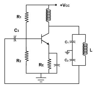
I just simulated this circuit in pSpice and it doesn't work - just look at the transistor bias voltage.
I agree with the opinion that this page doesn't explain how the circuit works - I'm no electronics newbie but I'm new to this circuit and for the first time, Wiki hasn't given me enough to get started with. I'll be back with edits once I've got my head round things.Fishtrousers (talk) 03:13, 14 September 2011 (UTC)
- Hello, I think the biasing in Figure 3 (at the base of the transistor) should be explained in the overview, as I can't seem to find an explanation in the article as of 2014-08-14
- I've expanded it mildly but with references. I'd appreciate if anyone more savvy could check it.
- 190.195.122.36 (talk) 03:39, 14 August 2014 (UTC)
- The biasing is straightforward: the resistive divider R3-R2 puts about 3 V on the base. The transistor's VBE drop will put the emitter at about 2.3 V, and emitter resistor R1 will set the collector current to about 1 mA.
- I don't like figure 3 for many reasons. There's no AC bypass shown for the tank current. At 1 mA, rE will be about 30 ohms; the tap will transform that to 120 ohms across the coil. At 50 MHz, the reactance of 150 nH is 2 π 50 MHz 150 nH = 47 ohms. Consequently, the resonator is heavily loaded.
- I looked on the web for better designs, but I came up dry.
- An old Army text explains, "For minimum feedback loss, the ratio of the capacitive reactance of C1 to C2 should be approximately equal to the ratio of the output impedance to the input impedance of the transistor."[1] I think that statement isn't quite right, but C2 should larger than C1.
- I'd also run at a higher bias current to get a better fT, but that triggers other problems.
- I just don't like figure 3.
- Glrx (talk) 23:49, 17 August 2014 (UTC)
Glrx, I agree that decreasing the size of R1 will provide more accuracy in terms of frequency. However, I disagree that C2 should be bigger than C1 or that L1 is too big (if that is what you mean by overloading for L1). Try reducing R1 and using L1, C1 and C2 in the low micro range. Let me know if it works for you (I assume you use PSpice - I would be curious to know what version). If you can't get the simulation to work, I will give you the actual numbers I used. I got the equation to match my simulation at 125kHz.
I also looked on the Internet for other circuits. I simulated 5 or 6 of them including the ones in figures 1 and 2 but most of them didn't work, either because values of components are not given or because something is not shown in the schematic which prevents simulation from working like biasing (just like for figures 1 and 2 - I wonder what is the point of having a generic circuit without showing you how to bias the transistor). Out of all the circuits I simulated, the only one I got to work is the one in figure 3. I think we should ask User:Msiddalingaiah who uploaded the schematic where he got the image and if he simulated or built the circuit. The way the circuit looks does not work for me so I would think it's not practical with the current values of resistance, capacitance and inductance. Also, the frequency stated in the image does not matcth the frequency you get if you use the frequency equation. The image should be modified and replaced.
ICE77 (talk) 08:17, 14 August 2015 (UTC)
- Decreasing R1 will make things worse. My comment about C2 is essentially sourced to TM 11-690; the input impedance of an emitter at 1 mA is about 30 Ω and the output load impedance at the collector might be 1500 Ω (XL × Qloaded = 47 × 30). Consequently the TM would recommend C2 about 7 times C1. Getting a simulation to work says nothing about good design; oscillators will oscillate with very poor Qs. Glrx (talk) 02:47, 15 August 2015 (UTC)
I modeled this in Circuit Maker and it's nowhere near 50Mhz. I get 35Mhz at Vout and see about 150MHz dumped through C3. Papwalker (talk) 07:38, 1 January 2016 (UTC)
References
- ^ Basic Theory and Application of Transistors, Dover, 1963[1959], TM11-690
LTspice shows it oscillating near 1.6 MHz. — Preceding unsigned comment added by 71.171.44.231 (talk) 18:41, 27 December 2016 (UTC)
- for me it oscillates at 48 MHz in ltspice; maybe you aren't using realistic parasitic properties? i also used a load > 150 ohm -- Waveguy (talk) 23:53, 5 July 2018 (UTC)
-2017-02-27-
I modeled this circuit in LTSpice and it doesn't start with these values with 2N2222 transistor. I started to changing values and yes, it oscillate with 100uH and 100nF, 100nF (some audio frequencies and few-MHz also). BUT adding any parasitic series resistance to model a real world, non-ideal parts, makes this circuit more "stable" and oscillations are gone. I did this circuit quickly on a breadboard in "dead-bug" style. It doesn't work with two transistors BC546 and old UL1000 (polish '70s (early integrated circuit) part, which contains 4 NPNs and two of them can be accessed directly). Checked all parts, all connections few times. After I changed transistor I did this circuit again and still doesn't work even if I experimented with more and more values of caps and inductors. My oscilloscope was showing no oscillations but DC multimeter was showing DC voltages as on the same nodes in LTSpice. So, yes it works but only in simulation. And it works for DC. After few hours of this dissapointment I just want this circuit to be changed to something that works in real world. As Robert A. Pease wrote: My favorite programming language is ... solder.
2017-5-27
I just modeled with LTSpice and it is working. I gave initial conditions for inductor currents (0amps) and voltages(0volts) at capacitor nodes. It takes about 500us to get the oscilator to oscilate gradually. The delay is caused by 100nF capacitor is taking a while to get charged so that base of the transitor gets to its biasing voltage. I changed inductor values and checked the frequency and it is working according to the equation. — Preceding unsigned comment added by 123.231.67.106 (talk) 05:41, 27 May 2018 (UTC)
Added on 2017-5-27.
It seems if you use real inductor models and capacitor models, the oscillation amplitude is severely degraded. So be careful about series resistances of inductor and capacitors you use and also there seems to be a bug in LTSPice (ver. XVII) that real inductor models show a parallel resistance in the range of few 10s of ohms!!! — Preceding unsigned comment added by 123.231.67.106 (talk) 06:42, 27 May 2018 (UTC)
- An IRC contact of mine built this last night (using deabdbug construction) and it works. I modeled this just now in ltspice, adding parasitic properties ESR 0.01 ohm to each 100pF and 0.4 ohm to the inductor; and it works if the heaviest load is above about 150 ohm. maybe your trouble is due to evil breadboard parasitics or too heavy load? i suggest trying manhattan construction and put the circuit in a cage -- Waveguy (talk) 23:48, 5 July 2018 (UTC)
Added on 2018-8-8
Hey guys. It works in LTSpice just fine, just make sure not to start the simulation at "0". Set it to start at 1us (microsecond) and it will then work and you will see the waveform. This circuit layout definitely works for real since I built a exactly similar circuit with different values for 1Mhz on a breadboard and it oscillates perfectly on my scope, the waveform even looks as predicted. I suspect it's something to do with initial conditions or something LTSpice isn't happy about. Just start the simulation somewhere after zero seconds and it will work — Preceding unsigned comment added by 2601:1c1:8701:cc4e::eeb3 (talk • contribs) 19:05, 8 August 2018 (UTC)
- A bit late I know, but... This is easily explained. An oscillator works by feeding a signal from its output to its input. The issue is that there must be a signal to feed back. In a real circuit, the amplifying device introduces a small amount of noise into the tuned circuit plus there is also excitation from voltage disturbances during power up. It may be small, but it is large enough to excite the tuned circuit and cause it to feed back some signal which grows in magnitude until the amplitude maxes out (usually due to the loop gain falling below unity as the signal reaches the limits of the amplifier).
- In the case of any form of spice emulation, at t=0 the noise and any power up disturbance is missing, hence there is nothing to excite the tuned circuit. However advancing t a small amount creates a small DC offset which the amplifier attempts to feed back changing the input DC offset and away the circuit goes.
- If it were possible to build the circuit for real and eliminate all noise and any other input signal, the same effect would occur - no oscillation. Applying a small DC voltage to the amplifier would be enough to start it oscillating normally expected. Such a condition is not possible in the real world, only in theory. 86.146.209.237 (talk) 16:28, 3 June 2020 (UTC)
Basic Theory Description[edit]
The original text placed too much emphasis on the requirement of a capacitive feedback voltage divider. This is very misleading as the Colpitts oscillator does not require such a connection. Indeed, such a required connection was clearly contradicted by Fig 2, and the original patent drawing version. Kevin aylward (talk) 16:24, 26 December 2012 (UTC)
- The Colpitts is distinguished in that feedback is taken from a capacitive voltage divider across the inductor. The Clapp oscillator has a capacitive voltage divider, but it is not across the inductor; there is an extra capacitor in there. Fig. 2 of the Colpitts patent clearly shows a capacitor voltage divider connected to the tube's cathode. I changed the introductory text back. If you have doubts check the 4 citations at the end of the sentence. --ChetvornoTALK 19:48, 28 December 2012 (UTC)
The citations are irrelevant. What matters is, what does the actual patent schematic show to anyone that can actually understand the schematic’s operation for themselves. Sure, there are capacitors connected together, giving the notional of a tap, but this is purely illusionary. The schematic shows a standard connection of a Colpitts oscillator that can be topologically redrawn as I show here:

Noting that, as described in the patent, the schematic relies on their being an impedance in the power supply connection.
I agree that it is not clear from the patent schematic where the ground is, but the most rational place for it is at the cathode, forming what would be the equivalent of what is invariably referred to as the standard common emitter Colpitts oscillator, i.e. a capacitor from output to ground, a capacitor from input to ground, and a *feedback* *inductor* from output to input. Irrespective of the actual patent schematic, the shown schematic is indeed a Colpitts oscillator, and does not have a capacitor feedback tap. Therefore a Colpitts oscillator description should not imply that a voltage feedback divider is required, when it is clearly not.
Kevin Aylward — Preceding unsigned comment added by 82.21.243.129 (talk) 11:39, 1 January 2013 (UTC)
- Patent figure 2 clearly has the two capacitors (labeled 16 and 13). Figure 3 of the patent does not have capacitor 13, but the text of the patent explains that the capacity of antenna 28 is used in place of 13. Patent figure 1 shows a topological Clapp, but the text explains that capacitor 21 is a blocking capacitor (DC stopping) rather than a tuning capacitor. Glrx (talk) 18:04, 29 December 2012 (UTC)
Single Active Device[edit]
I have re-added in the information that the Colpitts oscillator uses only one active component. This was an absolutely crucial reason for the invention and patent of this particular oscillator. Many oscillators at the time had several tubes and consequently, were very expensive. A single tube was the key distinguishing feature of the Colpitts oscillator, and this should be noted, more so than the simple presence of two capacitors, and a single inductor. — Preceding unsigned comment added by Kevin aylward (talk • contribs) 11:44, 28 December 2012 (UTC)
- Do you have a source for a single tube being a distinguishing feature? My understanding is that early oscillators were all one tube affairs. The 1913 tickler oscillator was one tube. The single tube did not distinguish the 1918 Colpitts from the 1915 Hartley according to you.[1] There was a significant effort to put many functions into a single tube (e.g., oscillator and a mixer). Glrx (talk) 17:36, 29 December 2012 (UTC)
Practical circuit example[edit]
The practical circuit will need decoupling between 0v and the + side of the inductor else the power supply will form part of the tank circuit. In fact, it needs to be a low inductance, low resistance high capacitance (much higher than c1 and c2 in order not to load the tank circuit.Nick Hill (talk) 12:35, 9 August 2015 (UTC)
- It's not a "practical schematic"; power supplies are typically viewed as a perfect short. Glrx (talk) 03:02, 15 August 2015 (UTC)
- Agreed. But since it is described as practical, and since a modification makes the design realisable using practical components (I have built this design with real components) it would be only fair to demonstrate the supply as decoupled. This could have an added benefit of making the tank circuit structure more obvious to those with less EE experience. Nick Hill (talk) 22:21, 19 August 2015 (UTC)
- The practical example has now a capacitor between power supply and ground - as every RF engineer includes automatically. Simulation with LTSpice gives easy oscillation and breadboarding of circuit was immediate success, too. AndreAdrian (talk) 14:32, 20 February 2024 (UTC)
- Agreed. But since it is described as practical, and since a modification makes the design realisable using practical components (I have built this design with real components) it would be only fair to demonstrate the supply as decoupled. This could have an added benefit of making the tank circuit structure more obvious to those with less EE experience. Nick Hill (talk) 22:21, 19 August 2015 (UTC)
Comments and question[edit]
1. It would be nice to replace figures 1 and 2 with circuits that show the bias.
2. "If the two capacitors are replaced by inductors and magnetic coupling is ignored, the circuit becomes a Hartley oscillator. In that case, the input impedance is the sum of the two inductors and a negative resistance given by: .

In the Hartley circuit, oscillation is more likely for larger values of transconductance and larger values of inductance.
Interestingly, the above analysis also describes the behavior of the Pierce oscillator. The Pierce oscillator, with two capacitors and one inductor, is equivalent to the Colpitts oscillator. Equivalence can be shown by choosing the junction of the two capacitors as the ground point. An electrical dual of the standard Pierce oscillator using two inductors and one capacitor is equivalent to the Hartley oscillator."
All of the above information should not be in this article. It should be in the Hartley and Pierce oscillators articles.
3. For the equation , what is RL if there is an inductor at the collector?

ICE77 (talk) 08:53, 11 August 2015 (UTC)
Impractical circuit schematics[edit]
I don't think any of the circuits presented in this article are practical. The common-base BJT implementation does not show biasing (file:Cb colp.svg) and neither does the common-collector BJT implementation (file:Cc colp2.svg). I simulated both of the circuits in PSpice without any success. If any of you had success, I would like to know, especially how you implemented the hidden details and what component sizes you used.
The only circuit I got to work out of the ones shown in this article is the practical implementation of the circuit (file:NPN Colpitts oscillator collector coil.svg). However, as it is, it does not oscillate and the nominal frequency is actually higher if calculated with the frequency equation and compared to the number stated in the image. I changed L1, R1, C1 and C2 to actually get something to simulate at 125kHz.
Since Colpitts and Hartley oscillators are dual circuits of each other and most schematics show an inductor on the collector of the BJT for both circuits, I believe there is a more appropriate circuit schematic that I also simulated successfully (http://www.expertsmind.com/CMSImages/1892_colpitts%20oscillator.png). In a Colpitts oscillator two capacitors are typically center-tapped and in parallel with an inductor. The Hartley oscillator has two center-tapped inductors in parallel with a capacitor.
I think this article should show practical circuits. The circuits should be simple and they should not hide important details like biasing or gain.
ICE77 (talk) 20:37, 14 August 2015 (UTC)
- All the schematics look right; "typically center-tapped" is wrong. Glrx (talk) 03:00, 15 August 2015 (UTC)
The CB and CC schematics are too generic. They don't show biasing and using ideal current sources is just too easy.
I used "center-tapped" because it's the only way I can explain two capacitors that are joined together and shorted to ground. Maybe there is a better expression. If there is, I don't know what it is.
ICE77 (talk) 23:55, 26 August 2015 (UTC)
The first question is: do we need practical circuits? This is not a guide on how to build a practical circuit but an article on what a Colpitts oscillator is and what distinguishes it from other oscillator circuits. In that respect, a circuit without component values would be adequate to the task. I would say that a circuit where the inductor is not visibly in parallel with the capacitor divider might confuse readers who are not familiar with the concept that the power supply is a short circuit (to AC).
A better circuit would be one where the tuned circuit is a clear and obvious parallel circuit. If the circuit has to be practical then this one might be a better choice. I just knocked it up on a breadboard, though with a different transistor (2N3704) and a 10 micro Henry inductor and it oscillated nicely at 782 kHz. I did use ceramic capacitors which is probably why the frequency is a tad higher than it should be.
The Hartley version is here, and this one works as well though, as they suggested, I did have to replace R3 with a pot and adjust for best output. --Elektrik Fanne 13:43, 25 March 2016 (UTC)
- The article should have simplified schematics, but I'm not opposed to providing a complete schematic.
- Please do not assume that a working circuit implies a good design.
- Quick estimates show that both common-base circuits you linked are poor designs.
- Both circuits claim an emitter current of around 20 mA, so the impedance looking into the base is about 1.5 ohms. The Colpitts circuit puts 1.5 × 42 = 24 ohms across the tank. The Hartley circuit puts 1.5 × 62 = 54 ohms across the tank. A 3.3 μH ind at 1 MHz has a reactance of about 20 j ohms. A 10 nF cap at 0.5 Mhz has a reactance of about −32 j ohms. Welcome to the world of pathetic-Q oscillators; the designs ignore resonator loading.
- It gets worse. With a Q of 100, the tanks should have a parallel loss resistance of more than 2 kilohms. Driving 20 mA through that loss resistance produces 40 V peak -- but there's only 6 to 9 V of head room in the designs (and good designs will keep VCE > 2 V). Component selection is off by an order of magnitude.
- That's why WP wants reliable sources rather than somebody's blog or personal website. Glrx (talk) 18:11, 25 March 2016 (UTC)
- Is this an article on Colpitts oscillator or is it an article on how to design a good Colpitts oscillator? I don't think it matters how good or bad a particular design is as long as demonstrates the esential features. Why not just use the circuit and leave out the component values? I also don't see why any particular circuit has to exist in a reference somewhere, as it is the features of the circuit that require references. The circuit itself is just a visual aid. The reason I would prefer a circuit where the tuned circuit is visibly a parallel circuit is because shortly after I corrected the type of resonant circuit from series to parallel over at Ignition system, the very next day, someone challenged it on the talk page. --Elektrik Fanne 12:10, 26 March 2016 (UTC)
- Old thread, I know. I think it would be wrong to leave out components values. Exact values may not be very relevant but values in the ball park are essential to the understanding of how a circuit works. In the extreme we could consider how a 0 Ohm or 100M Ohm would change a circuit making it work (or not work) totally differently and one could argue that if a circuit does not work is the circuit at all that it purports to be. — Preceding unsigned comment added by 185.147.20.2 (talk) 10:26, 22 January 2021 (UTC)
- Is this an article on Colpitts oscillator or is it an article on how to design a good Colpitts oscillator? I don't think it matters how good or bad a particular design is as long as demonstrates the esential features. Why not just use the circuit and leave out the component values? I also don't see why any particular circuit has to exist in a reference somewhere, as it is the features of the circuit that require references. The circuit itself is just a visual aid. The reason I would prefer a circuit where the tuned circuit is visibly a parallel circuit is because shortly after I corrected the type of resonant circuit from series to parallel over at Ignition system, the very next day, someone challenged it on the talk page. --Elektrik Fanne 12:10, 26 March 2016 (UTC)
External links modified[edit]
Hello fellow Wikipedians,
I have just modified one external link on Colpitts oscillator. Please take a moment to review my edit. If you have any questions, or need the bot to ignore the links, or the page altogether, please visit this simple FaQ for additional information. I made the following changes:
- Added archive https://web.archive.org/web/20140814113015/http://www.ijeat.org/attachments/File/v2i5/E1662062513.pdf to http://www.ijeat.org/attachments/File/v2i5/E1662062513.pdf
When you have finished reviewing my changes, you may follow the instructions on the template below to fix any issues with the URLs.
This message was posted before February 2018. After February 2018, "External links modified" talk page sections are no longer generated or monitored by InternetArchiveBot. No special action is required regarding these talk page notices, other than regular verification using the archive tool instructions below. Editors have permission to delete these "External links modified" talk page sections if they want to de-clutter talk pages, but see the RfC before doing mass systematic removals. This message is updated dynamically through the template {{source check}} (last update: 18 January 2022).
- If you have discovered URLs which were erroneously considered dead by the bot, you can report them with this tool.
- If you found an error with any archives or the URLs themselves, you can fix them with this tool.
Cheers.—InternetArchiveBot (Report bug) 00:32, 11 August 2017 (UTC)
Practicality of circuit in diagram[edit]
The circuit has the inductor connected to the positive rail which has no RF decoupling at all. The positive rail should have a capacitor (0.01 uF) connected between it and common negative. This allows the current that is circulating between inductor and the two capacitors to do so without having to go through the power supply. In the real world, this can make the difference between the circuit oscillating and not oscillating. This is also the reason why it should not be a practical circuit - it is incomplete. — Preceding unsigned comment added by 2600:1700:CD40:C510:5CFC:C486:54E6:F04C (talk) 05:56, 30 January 2022 (UTC)
- Added capacitor parallel to battery, added load resistor, removed "dubious" flag. AndreAdrian (talk) 12:55, 17 February 2024 (UTC)
Why no tubes?[edit]
It seems odd that right after saying it was invented in 1918, we start giving examples of transistor circuits. Wouldn't it make more sense to start with a tube circuit and then segue into the more modern implementations? RoySmith (talk) 19:19, 30 January 2024 (UTC)